
On this page · 9 sections
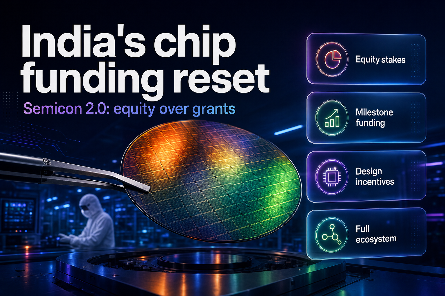
Summary. On 15 July 2026 the Union Cabinet approved Rs 1.27 lakh crore (Rs 1.27 trillion) for the second phase of the India Semiconductor Mission, ISM 2.0, as part of a combined Rs 1.9 trillion package that also set aside Rs 62,500 crore for a revamped Mobile Phone Manufacturing Scheme. The change that matters most for founders is structural, not the headline number: the government is moving away from the flat grants of phase one toward a grant-plus-equity model for chip-design startups and a co-investment or royalty-linked structure for larger firms, according to Union Electronics and IT Minister Ashwini Vaishnaw. Fab incentives were cut from a flat 50% in ISM 1.0 to 40% for silicon fabrication and 35% for display and compound-semiconductor units, while equipment, chemicals, gases and materials makers get up to 30% of project cost and research and talent programmes get combined central and state support of up to 75%. The government expects ISM to catalyse Rs 4 trillion of investment, Rs 2 trillion of production and Rs 1 trillion of exports. As of 15 July 2026, phase one had already approved 12 projects worth more than Rs 1.60 trillion. This analysis explains the new funding mechanics and what a deep-tech founder should do about them.
What changed on 15 July 2026
The Cabinet cleared two initiatives on the same day. ISM 2.0 received Rs 1.27 lakh crore, and the Mobile Phone Manufacturing Scheme received Rs 62,500 crore, for a combined outlay of nearly Rs 1.9 trillion, as reported by Business Standard. Phase one, approved in December 2021, ran on a Rs 76,000 crore framework that offered fiscal support of up to 50% and was aimed almost entirely at chip manufacturing. Phase two widens the aperture to the whole value chain.
"The semiconductor industry is a foundational industry. All devices we use need semiconductor chips. The entire electronics value chain has now been covered," Vaishnaw said while announcing the decision. In plain terms, ISM 2.0 pays not just for fabs and packaging plants but for the design houses, equipment makers, specialty-chemical and gas suppliers, materials firms, research groups and training programmes that a real ecosystem needs. Detailed operational guidelines and the scheme framework are due within a fortnight of the announcement, so the specifics founders will apply against are still landing.
The funding model has flipped
Phase one wrote cheques. A qualifying project got a fixed percentage of its capital expenditure back as a grant, disbursed on a pari passu basis as milestones were met. Phase two keeps that logic for large fabrication and packaging projects but introduces something new for the design layer where most startups actually sit.
For smaller startups designing strategic and commercial chips, the government has proposed a grant-plus-equity funding model, with the stated goal of keeping the intellectual property created inside the country. For medium-sized and large domestic companies entering strategic and commercial chip design, it has proposed a co-investment or royalty-linked funding and incentive structure. Reporting from Communications Today and channeliam indicates the state intends to take minority stakes rather than control, but the precise equity terms, caps and exit mechanics will only be clear when the operational guidelines are published.
| Applicant type | ISM 2.0 funding model | What it means in practice |
|---|---|---|
| Chip-design startup | Grant plus equity | Non-dilutive grant paired with a state equity stake; IP stays in India |
| Medium or large design firm | Co-investment or royalty-linked | Government shares upside via co-investment or royalties, not a pure grant |
| Fabrication unit | Recalibrated capex incentive | Up to 40% for silicon fabs, 35% for display and compound |
| Equipment, chemicals, gases, materials | Flat incentive | Up to 30% of project cost |
| R&D and talent programmes | Combined central and state support | Up to 75% of project cost |
The equity turn is the headline for founders. A grant dilutes nobody; equity does. The trade is access to patient capital that most Indian deep-tech companies cannot raise from venture funds alone, given the long timelines and heavy capital needs of silicon. Whether the terms are founder-friendly is the question the guidelines have to answer.
Recalibrated incentives, activity by activity
The rate cuts are not a retreat. They reflect an ecosystem that now exists and no longer needs to pay a first-mover premium. As one government official quoted by Business Standard put it, the incentive structures "had to be brought down now that we have an ecosystem" of approved units, freeing funds to attract more players rather than over-subsidise a few.
| Activity | ISM 1.0 incentive | ISM 2.0 incentive |
|---|---|---|
| Silicon semiconductor fabrication | Flat 50% | 40% |
| Display and compound-semiconductor fabs | Flat 50% | 35% |
| Advanced packaging (ATMP/OSAT) | Flat 50% | 35% |
| Conventional packaging | Flat 50% | 25% |
| Equipment, chemicals, gases, materials | Not a distinct track | Up to 30% |
| R&D in advanced nodes; talent programmes | Not a distinct track | Up to 75% (centre plus state) |
The most generous number in the whole scheme, up to 75% combined central and state support, sits on research and talent, not on fabrication. That is a deliberate signal: India is spending most aggressively where it is furthest behind, on the design IP and the engineers, rather than on more assembly lines.
Where India Semiconductor Mission 1.0 actually got to
Founders should read Semicon 2.0 against what phase one delivered, because the base is stronger than the sceptics expected. As of 15 July 2026 the government had approved 12 projects with a cumulative investment of more than Rs 1.60 trillion under the Rs 76,000 crore first phase. The anchor projects are real and moving:
Micron's Rs-denominated ATMP facility in Sanand, Gujarat, cleared in June 2023, carried a $2.75 billion price tag and was the first project approved. The Tata group's fabrication joint venture with Taiwan's Powerchip Semiconductor Manufacturing Corporation, at about $11 billion, is the only true wafer fab among the approved projects. On the packaging side, CG Power and Kaynes Semicon have both brought OSAT capacity online in Gujarat, with Kaynes reaching commercial production in 2026.
The design ecosystem, which is where Semicon 2.0 concentrates its new firepower, also has a track record. Under the Design Linked Incentive scheme, as of January 2026 the programme supported 24 semiconductor design startups that had together attracted nearly Rs 430 crore in venture capital. The national Electronic Design Automation platform had logged roughly 2.25 crore tool hours across about 67,000 students and more than 1,000 startup engineers. Startups had completed 16 tape-outs yielding six chips at advanced foundry nodes, including 12 nm. The next-phase target is at least 50 fabless companies. India is also building sovereign processor IP, including the DHRUV64 64-bit chip from C-DAC and the wider SHAKTI, AJIT and VIKRAM families on the open RISC-V architecture, which matters because India consumes close to 20% of global microprocessor output.
What Semicon 2.0 means for deep-tech founders
Four practical takeaways follow from the design above.
First, if you are a chip-design startup, the calculus is no longer grant-or-nothing. You can pair a non-dilutive grant with state equity, which lengthens your runway through the multi-year gap between tape-out and revenue that kills most fabless companies. Model the dilution carefully against what the same milestone would cost in venture equity, and wait for the operational guidelines before assuming the state's terms beat a private round.
Second, the IP-retention condition is the string attached. The grant-plus-equity model exists so that strategic chip IP stays in India. Founders planning offshore holding structures or foreign acquisition exits should read the fine print, because the funding is designed to keep ownership domestic.
Third, the biggest subsidy is on people and research, not silicon. A startup that structures part of its work as advanced-node R&D or as a talent programme can access up to 75% combined central and state support. For a capital-light design or EDA-adjacent company, that is a more accessible door than the fab track.
Fourth, timing is now. Guidelines are due within a fortnight of the 15 July announcement, and incentives are disbursed pari passu against milestones, so applications that are ready with clear, verifiable milestones will move first. This is the same discipline that rewards teams building on the IndiaAI Mission and India's sovereign-AI push: the funding favours execution-ready plans over ambition.
For the wider hardware and manufacturing base, Semicon 2.0 pulls demand through to the firms around silicon, from smart-manufacturing and IoT deployments in Indian factories to the physical-AI and robotics systems that will run on domestically made chips.
The global backdrop
The reset is a response to geopolitics as much as economics. Taiwan alone produces over 60% of the world's semiconductors and close to 90% of the most advanced chips, a concentration that the COVID-era shortages, which hit more than 169 industries, exposed as a systemic risk. The United States, the European Union, Japan and South Korea have all launched national chip programmes, and India is positioning as a trusted alternative node. Government projections put the Indian semiconductor market at $100 billion to $110 billion by 2030, up from about $38 billion in 2023, with a stated ambition to serve 70% to 75% of domestic chip demand by 2029 and to reach 3 nm and 2 nm nodes on the Semicon 2.0 roadmap. Export controls remain the wildcard, which is why founders should track the chip export-control and model-restriction risks that could reshape supply access mid-project.
Pankaj Mohindroo, chairman of the India Cellular and Electronics Association, framed the moment this way: "India has demonstrated the intent and long-term commitment to the semiconductor industry with more than 12 approved projects in just four years. ISM 2.0 now builds on this strong foundation with a significant emphasis on design, R&D, capital goods, and entire supply chain and skill development." The strategy is clear. The terms that decide whether founders win from it are still a fortnight away.
FAQ
How eCorpIT can help
eCorpIT is a senior-led engineering organisation in Gurugram that builds the software, AI and cloud layers that sit on top of silicon, from device and firmware-adjacent applications to the data platforms and AI workloads that hardware startups ship around their chips. We help Indian deep-tech and product teams turn a funded roadmap into working systems, and we design those systems to align with the DPDP Act and India's data-localisation expectations. If you are building in the semiconductor or wider deep-tech ecosystem and need a delivery partner for the digital layer, contact us.
References
- Press Information Bureau. "India Semiconductor Mission 2.0." Government of India, 2026.
- Aashish Aryan. "Cabinet unveils Rs 1.9 trillion semiconductor, smartphone manufacturing plans." Business Standard, 15 July 2026.
- Business Standard. "Cabinet clears Rs 1.28 trn ISM 2.0, approves Rs 62,500 cr for mobile scheme." 15 July 2026.
- The Federal. "Cabinet approves Semiconductor Mission 2.0 worth Rs 1.2 lakh crore." 2026.
- Communications Today. "Centre to take equity stakes in chip startups under Semicon 2.0." 2026.
- channeliam. "Govt Plans Equity Funding for Chip Startups." 17 July 2026.
- India Briefing. "India's Semicon 2.0 Opens New Frontiers for Global Semiconductor Firms." 2026.
- India Semiconductor Mission. "Official portal." Government of India.
- CRN Asia. "Kaynes Semicon starts production at Sanand OSAT facility." 2026.
- APAC News Network. "Centre Approves India Semiconductor Mission 2.0 with Rs 1.27 Trillion Investment Plan." July 2026.
- Semicon Hunt. "India Launches Semiconductor Mission 2.0." 2026.
_Last updated: 18 July 2026._